- 您现在的位置:买卖IC网 > Sheet目录370 > ZXGD3105N8TC (Diodes Inc)IC SYNCH MOSFET CNTLR SO8
�� �
�
�A� Product� Line� of�
�Diodes� Incorporated�
�ZXGD3105N8�
�Application� Information� (cont.)�
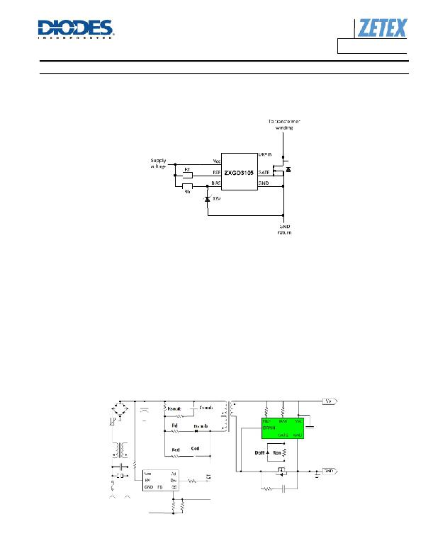
�Layout� Guidelines�
�When� laying� out� the� PCB,� care� must� be� taken� in� decoupling� the� ZXGD3105� closely� to� V� CC� and� ground� with� 1� μ� F� low-ESR,� low-ESL� X7R� type�
�ceramic� bypass� capacitor.� If� the� converter’s� output� voltage� is� higher� than� 20V,� a� 12V� zener� diode� should� be� connected� from� the� bias� pin� to� GND� to�
�clamp� the� Gate� voltage� and� protect� the� synchronous� MOSFET.� Figure� 7� shows� the� typical� connection� diagram.�
�Figure� 7� Zener� Voltage� Clamp� Arrangement�
�GND� is� the� ground� reference� for� the� internal� high� voltage� amplifier� as� well� as� the� current� return� for� the� gate� driver.� So� the� ground� return� loop�
�should� be� as� short� as� possible.� Sufficient� PCB� copper� area� should� be� allocated� to� the� Vcc� and� GND� pin� for� heat� dissipation� especially� for� high�
�switching� frequency� application.�
�Any� stray� inductance� involved� by� the� load� current� may� cause� distortion� of� the� drain-to-source� voltage� waveform,� leading� to� premature� turn-off� of�
�the� synchronous� MOSFET.� In� order� to� avoid� this� issue,� drain� voltage� sensing� should� be� done� as� physically� close� to� the� drain� terminals� as�
�possible.� The� PCB� track� length� between� the� controller� Drain� pin� and� the� MOSFET’s� terminal� should� be� kept� less� than� 10mm.� MOSFET� packages�
�with� low� internal� wire� bond� inductance� are� preferred� for� high� switching� frequency� power� conversion� to� minimize� body� diode� conduction.�
�After� the� primary� MOSFET� turns� off,� its� Drain� voltage� oscillates� due� to� reverse� recovery� of� the� snubber� diode.� These� high� frequency� oscillations�
�are� reflected� across� the� transformer� to� the� Drain� terminal� of� the� synchronous� MOSFET.� The� synchronous� controller� senses� the� Drain� voltage�
�ringing,� causing� its� gate� output� voltage� to� oscillate.� The� synchronous� MOSFET� cannot� be� fully� enhanced� until� the� Drain� voltage� stabilizes.�
�In� order� to� prevent� this� issue,� the� oscillations� on� the� primary� MOSFET� can� be� damped� with� either� a� series� resistor� Rd� to� the� snubber� diode� or� an�
�R-C� network� across� the� diode� (refer� Figure� 8).� Both� methods� reduce� the� oscillations� by� softening� the� snubber� diode’s� reverse� recovery�
�characteristic.�
�Figure� 8� Primary� Side� Snubber� Network� to� Reduce� Drain� Voltage� Oscillations�
�ZXGD3105N8�
�Document� Number� DS35101� Rev.� 3� -� 2�
�12� of� 14�
�www.diodes.com�
�March� 2013�
�?� Diodes� Incorporated�
�发布紧急采购,3分钟左右您将得到回复。
相关PDF资料
ZXLD1100H6TA
IC LED DRVR WHITE BCKLGT SC-70-6
ZXLD1101ET5TA
IC LED DRVR WHITE BCKLGT SOT23-5
ZXLD1320DCATC
IC LED DRVR WHITE BCKLGT 14-TDFN
ZXLD1321DCATC
IC LED DRVR WHITE BCKLGT 14-TDFN
ZXLD1322DCCTC
IC LED DRIVR WHITE BCKLGT 14-DFN
ZXLD1350ET5TA
IC LED DRIVR WHITE BCKLGT TSOT-5
ZXLD1352ET5TA
IC LED DRIVER HIGH BRIGHT TSOT-5
ZXLD1356DACTC
IC LED DRIVER WHITE BCKLGT 6-DFN
相关代理商/技术参数
ZXGIF11
制造商:OMRON AUTOMATION AND SAFETY 功能描述:INTER UNIT NPN (RS232 TO BIN) 制造商:OMRON Industrial Automation 功能描述:INTER UNIT NPN (RS232 TO BIN)
ZX-GIF11
功能描述:INTER UNIT NPN (RS232 TO BIN) RoHS:是 类别:传感器,转换器 >> 配件 系列:* 标准包装:1 系列:* 其它名称:Y92EEG18T
ZXGIF11A
制造商:OMRON AUTOMATION AND SAFETY 功能描述:INTER UNIT NPN W/SETUP S/W 制造商:OMRON Industrial Automation 功能描述:INTER UNIT NPN W/SETUP S/W
ZX-GIF11A
功能描述:INTER UNIT NPN W/SETUP S/W RoHS:是 类别:传感器,转换器 >> 配件 系列:* 标准包装:1 系列:* 其它名称:Y92EEG18T
ZXGIF41
制造商:OMRON Industrial Automation 功能描述:INTER UNIT PNP (RS232 TO BIN)
ZX-GIF41
功能描述:INTER UNIT PNP (RS232 TO BIN) RoHS:是 类别:传感器,转换器 >> 配件 系列:* 标准包装:1 系列:* 其它名称:Y92EEG18T
ZXGIF41A
制造商:OMRON Industrial Automation 功能描述:INTER UNIT PNP W/SETUP S/W
ZX-GIF41A
功能描述:INTER UNIT PNP W/SETUP S/W RoHS:是 类别:传感器,转换器 >> 配件 系列:* 标准包装:1 系列:* 其它名称:Y92EEG18T